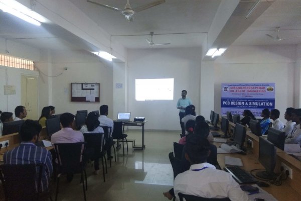
Workshop on “PCB Design & Simulation”
The Sharadchandra Pawar College of Engineering Organized two day’s Workshop on “PCB Design & Simulation” on January 24th & 25th, 2018 in association with Board of Student’s Development, Savitribai Phule Pune University, Pune.
- Title: Two day’s University Level Workshop on “PCB Design & Simulation”
- Event Date: 24/01/2018 & 25/01/2018
- Resource person:
- Sunny S. Hapse, Senior Developer, Esston Technology, Pune
- Swapnil V. Agawane, Junior Developer, Esston Technology, Pune
- Tajas R. Shilamkar, Design Engineer, Esston Technology, Pune
- Convener: Mahesh G. Chinchole
(Head Dept. of E&TC and Student Development Officer SPPU, Pune)
- Coordinator: Rahul S. Parbat, Prof. Vasudha. V. Patil
About workshop:
The workshop was conducted in collaboration with Esston Technology, from Pune. The company has a fast growth in PCB designing and Robotics. The company’s Chief Executive Mr. Sunny S. Hapse with Mr. Swapnil V. Agawane and Mr. Tajas R. Shilamkar conducted the workshop to guide the students in learning the technologies of the PCB Design & Simulation. They have taken about 16 hours of theoretical and practical sessions.
Mr. Sunny S. Hapse started the workshop with a very creative introductory session on 24th January 2018. First of all they have given the concepts which will be very helpful for designing the PCB practically, using some power point presentations. In this theoretical explanation part Mr. Sunny S. Hapse explained the Protious 8 and PAD 2 PAD software’s and the use of them for further practical implementation in designing the PCB. They have also given a brief idea about active and passive electronic components which are used in a PCB.
In the hands-on sessions, they have taken example of Arduino board PCB layout along with simulation. Power supply sections of Arduino board was designed and fabricated on 25th January 2018. The board was drilled with holes where the components were placed; the holes The hole should be in the size so that the terminal has to be freely placed in the hole.
The components were placed in the board have been soldered to the track so that the circuit is connected as per the design. After this step the engraved PCB will be ready to use.
Designed circuits were practically tested by means of conductivity and continuity of copper tracks, components placing and actual response of circuits was tested on multimeter.
- Duration: Two day’s workshop on January 24th & 25th, 2018
- of students attended this workshop: 26
- Topics covered in this Workshop:
- Introduction to Embedded System Design, Practical scenario, Protious 8 simulation Design (Circuit Diagram Implementation for power supply and any controller based board).
- Introduction to PAD 2 PAD design software. (Design Layout for 5V Power Supply).
- Practical Hands on PAD 2 PAD Software (Design Controller Based Layout).
- Practical Hands on PCB Development (PCB Printing, PCB Etching PCB Track Testing.
- Practical Hands on PCB Development (Component Mounting and Result Testing).
- Outcomes of attending the workshop:
- This workshop added new scopes to educate concepts and proficiency among the students in the field of PCB.
- Workshop has definitely enhanced the designing and development skills of the students which will give an advantage to them in their future.
- This Workshop gained students practical knowledge in the field of PCB Designing and Manufacturing and enhances their Creativity.
- Received large volumes of usable content within a compressed amount of time
- Students were designed and tested own Circuit.
- Learned design software like Protious 8 and PAD 2 PAD


